Return to Memolist
MMA Memo 166: The MMA Correlator
R. Escoffier
April 1, 1997
1) INTRODUCTION
This memo will describe the design of a correlator for the MMA. The MMA
project will likely begin in earnest in a few months, and the time has come to
start definite considerations for this large and expensive subsystem of the
array.
The design described here is for a lag correlator and justification for
this approach will be given. A system clock rate of 125 MHz is also chosen
and also justified. The decisions of system architecture and clock rate are
the most important to be made in selecting a correlator design and much
caution must be used before adopting the final approach.
At this time, no consideration will be given to the Atacama array (the
combined MMA and Japanese LMSA), and the design described will be a correlator
for the MMA alone. As plans and specifications for the Atacama array develop,
the MMA correlator design will be reconsidered.
2) CORRELATOR SPECIFICATIONS
This section gives a summary of the MMA correlator specifications.
Detailed system specifications will be developed over the next few months, and
this section will provide a starting point for this effort. The basic
starting specs for the correlator are:
| 40 | antennas |
| 8 | IFs per antenna (maximum bandwidth/antenna = 16 GHz) |
| 4 | GHz maximum sampling rate per IF |
| 2 | bit, 4 level sampling |
| 1024 | lags per baseline with a 2-GHz bandwidth, minimum |
| 4 | product pairs (RR, RL, LR, LL) possible for polarization |
| 30 | KM maximum baseline delay range |
3) JUSTIFICATION OF THE LAG ARCHITECTURE
Up to this point in considering designs for the MMA correlator, both lag
and FX architectures have been studied. NRAO has experience in both types of
systems for large arrays, having previously built the VLA with its lag
correlator and the VLBA with its FX correlator. The text below attempts to
justify the selection of the lag approach for the MMA correlator.
The MMA correlator will be a very large and expensive system as
correlators for astronomical instruments go. Conventional wisdom has it that
for small systems a lag correlator is most economical, but as an array
acquires more antennas, the FX approach will eventually become less expensive.
This is because, for a lag correlator, much of the hardware required varies as
the square of the number of antennas, whereas for the FX approach, much of the
logic (specifically, the FFT engines) increases linearly with the number of
antennas. This consideration, however, applies only to the silicon component
of the hardware and other requirements must be studied.
The table below compares the lag and FX correlator designs for the MMA
application. This table assumes:
- a system clock rate of 125 MHz (see Section 4).
- a custom lag correlator chip with a 4 X 4 X 2 matrix of correlators
(4 ant. by 4 ant. by 2 polarizations, see
Figure 4).
- a custom FX chip that will do one radix 8 FFT butterfly.
- a custom FX cross multiply chip with a 4 X 4 matrix of multipliers.
- FFT-to-cross multiply interface of 12 wires (4-bit real, 4-bit
imaginary, and a 4-bit exponent) at ½ the clock rate.
| parameter | lag correlator | FX correlator |
|---|
| custom chip designs | 1 | 2 |
| number of custom chips (station) | 0 | 30,720 [1] |
| number of custom chips (cross mult) | 12,800 [2] | 12,480 [3] |
| number of signal cables [*] | 0 | 20,480 [4] |
| number of signal cables [+] | 20,480 [4] | 61,440 [5] |
| [*] | between the delay lines and the FFT engines. |
| [+] | between the FFT engines or delay lines and the cross multipliers. |
| |
| |
| [1] | 40 ant. X 8 IFs X 32 parallel paths X 3 chips per FFT. |
| [2] | (40 X 40) X 8 IFs X 32 parallel paths / 16 corr per chip / 2 polz per chip. |
| [3] | (40 X 39)/2 X 8 IFs X 32 parallel paths / 16 circuits per chip. |
| [4] | 40 ant. X 8 IFs X 2 bits per sample X 32 parallel paths. |
| [5] | 40 ant. X 8 IFs X 12 bits per point X 32 parallel paths / 2 (½ clock rate). |
The advantages of the lag correlator are clear from this table:
- The FX correlator would require 2 custom chip designs, one for the
FFT and one for a matrix of cross multipliers, whereas the lag
design requires only one chip.
- The FFT butterfly chip would be very complex (at least 16-bit
arithmetic at 125 MHz is required) and would probably take at least
one year longer to develop than would the much simpler (but probably
larger) lag correlator chip.
- The amount of 125 MHz inter-stage wiring is much higher for the FX
design than for the lag correlator. The FX design will require over
80,000 cables whereas the lag system requires only a little over
20,000 (to put this in perspective, 80,000 125 MHz signal cables is
a factor of 380 times the VLA correlator requirement). In addition,
the number of signal cables given in the table above represents a
minimum. In order to achieve this minimum number of signal wires,
the cross multiplier matrix must be built in such a compact fashion
that no output of the station logic is required to drive more than
one cable. As will be seen in Section 5, this requirement can
probably be met with the lag design. However, the FFT output of the
FX design requires many more signals to drive the cross multipliers
and, because of the limitations of I/O pins in the cross multiplier
cards, a minimum wire interconnect will probably not be possible for
the FX. If this minimum condition is not met, the FX cable
requirements becomes more than 140,000 cables.
The number of signal cables is by far the most important factor in
determining the practicability of the MMA correlator. The number of wires can
be controlled by increasing the interface clock rate but at the cost of
requiring more expensive cables and larger, more expensive, connectors.
Section 4 will argue that a 125 MHz system clock rate is optimum for the MMA
correlator.
Neither custom chip postulated for the FX design would be very large.
If not for the large I/O requirements, higher levels of integration could be
considered to make the FX approach more attractive (at least from the silicon
standpoint). Still, the silicon utilization efficiency of the FX custom chips
would not be as high as for a large lag correlator chip. The simple and
regular nature of the lag correlator layout allows more efficient use of the
surface area of the chip.
Additional disadvantages of the FX system include the much more
complicated control logic requirements (for supplying the trig tables and
timing signals, etc. for hundreds of FFT cards). This additional complexity
will result in a longer development schedule and in a longer time to bring the
system to operational status (as was experienced with the VLBA correlator).
4) SYSTEM CLOCK RATE
The MMA correlator will be a very large system by any standards. Based
on just the bandwidth and number of baselines, it will have 178 times the
capacity of the VLA correlator. The maximum sample rate to be used in the
system will be 4 GHz. Since there is no practical way to handle this high
clock rate in such a large system, a lower clock rate parallel design must be
considered. The selection of the system clock rate is of extreme importance.
This decision will determine the final cost, size, reliability and operation
power requirements of the system, and it is important to select a design that
will optimize all of these considerations to the extent possible at the onset.
The table below gives a list of several possible selections for the
system clock rate, the number of resulting signal wires between the samplers
and the delay lines, and other considerations (the lag correlator design is
now assumed):
| system clock | wires from samplers | possible interface medium | possible logic family | comment |
|---|
| 4 GHz | 640 | individual coax | - | impractical |
| 2 GHz | 1,280 | individual coax | - | impractical |
| 1 GHz | 2,560 | individual coax | - | impractical |
| 500 MHz | 5,120 | individual coax | GaAs? | - |
| 250 MHz | 10,240 | multi-signal coax | ECL 100K | - |
| 125 MHz | 20,480 | multi-signal cable | ECL 10K | VLA technology |
| 62 MHz | 40,960 | multi-signal cable | ECL 10K | - |
| 31 MHz | 81,920 | twisted pair | TTL 74F | VLBA technology |
In this table, the term multi-signal cable refers to a medium such as the Gore
flat cable used in the VLA correlator. This cable can fit eight 50 ohm
transmission lines in a flat cable about 0.5 inches wide and costs about $10
for a 5-foot terminated 8-signal cable. The multi-coax cable term refers to a
medium such as AMP coaxial ribbon cable (AMP p/n 226581-9). This cable fits
eight 50 ohm coax lines into a flat cable about 0.8 inches wide and costs
about $40 for a 5-foot terminated cable.
In addition to the wiring technology, applicable logic families for
each design are given in the table above.
To minimize the cost and size of the correlator, one wants to select
from the table above the highest system clock rate which retains a convenient
IC logic family, inexpensive and compact interconnect cables and straight
forward printed circuit card technology.
A low clock rate, such as 31 MHz, would use very inexpensive
interconnect cable (twisted pair), but it has the disadvantage of requiring
many parallel paths. Also, the 74F TTL logic family is not good at driving
terminated transmission lines. This inability to drive low impedances makes
the rack-to-rack signal drive difficult and also makes printed circuit card
design more difficult because long unterminated lines on a card must be
avoided.
Higher clock rates, such as 250 MHz, require expensive and bulky signal
cables. Expensive and poorly supported logic families, like the ECL 100K
family, as well as more critical pc card design would also be required.
Based on previous NRAO correlator design experience, the highest clock
frequency in the table above for which a convenient logic family, inexpensive
interconnect cables, and simple pc card technology exists is at 125 MHz.
Hence, this clock rate is chosen for the MMA correlator design.
5) SYSTEM BLOCK DIAGRAM
A simplified block diagram for the MMA correlator is given in
Figure 1.
This diagram presents a fairly conventional lag correlator.
The analog outputs of the IF system drive sampler inputs where 2-bit,
4-level sampling is done at 4 GS/S. A block diagram of a sampler is seen in
Figure 2.
Some cost saving can be realized by making dual samplers that share
parts of the circuitry such as the phase lock loop and the sample clock phase
shift. This configuration means that a small residual delay error between two
IFs of the same antenna would have to be removed in software.
Logic in the mode selection block routes the sampler outputs into the
delay system. When fewer than 8 samplers per antenna are being used, this
stage will assure high system efficiency by replicating active sampler outputs
into unused delay lines and, hence, into otherwise unused correlators where
additional lags can be generated. In this way, maximum performance will be
obtained for the observational mode desired.
Next, delay lines are provided to phase the signals. The delay will be
provided in very efficient high density RAMs. For a 30 KM delay range,
524,288 RAM bits per sampler output bit is required.
The data format conversion block seen in
Figure 1 will take the 32
parallel outputs of each sampler and, using RAMs, re-sort the samples. Thus,
the 32 parallel outputs of a high-speed sampler would be converted from each
carrying every 32nd sample to each carrying short (about 1 msec) bursts of
contiguous samples. If the N-wide parallel (2-bit) output of a high-speed
sampler (each output carrying every Nth sample) were to drive the correlators
directly, an N-by-N matrix of correlators would be required so that every
sample gets correlated with every other sample. For N = 32, this would mean a
matrix of 1024 small correlators to correlate the output of every IF of every
baseline (each 8-lags in length).
By using the proposed format conversion scheme, the 32-wide parallel
output from a high-speed sampler will be transformed into 32 parallel signals
each carrying 1 msec segments of time contiguous samples that need only drive
an N-by-1 array of correlators. This simplification in the correlator
requirements is obtained at the cost of an inefficiency of about 0.2% which
results because the end bits in adjacent 1 msec time segments of samples will
never be correlated with each other.
Block diagrams (not shown) for the delay line and a data format
conversion card are almost identical, and it is possible that these two cards
can be of a single design. This design would have re-programmable logic such
as field programmable logic arrays that would be configured at power up for
one or the other function.
The cross correlator matrix of
Figure 1 is used to correlate the sampler
outputs of each antenna with those of every other antenna. At the
intersection of any antenna X with another antenna Y in this matrix, there
will be a 256-lag correlator. This correlator will compute lag products for
the XY baseline, while the antenna Y and antenna X intersection of the matrix
will compute the baseline lead products. Auto correlation products for each
antenna are obtained from correlators on the matrix diagonal.
Figure 3 gives a possible layout for the
correlator card. (The two axes of the correlator matrix in
Figure 3 are described as the "prompt" and
"delayed" inputs.) In order to minimize the delay line-to-cross
multiplier cable interconnect, a very compact cross correlator matrix
is essential. The design of Figure 3
places an entire 40 X 40 cross correlator matrix for two IFs of
opposite polarization on a single printed circuit card. This PC card
in addition is configured such that no signal drives more than one
load.
Each chip passes along its input signals to adjacent chips in a matrix
fashion. Column drive signals pass up through each column from the card input
pins and row drive signals come up a column to the diagonal of the matrix and
then drive in each direction to the entire row. Small programmable delay
lines will be required at the input to each internal correlator to insure that
all signals are phased to the correct bit regardless of the length of the path
required to reach the correlator.
The correlator card layout of
Figure 3 has one serious problem. The
125 MHz clock for two adjacent chip columns must be kept properly phased so
that two chips high up in the column can exchange signals. It is possible
that a very fast chip design will accommodate this requirement. Otherwise, a
slightly more complicated clock distribution will be required.
Figure 4 shows a block diagram of the
proposed custom lag correlator chip. This chip has a dual 4-by-4
array of correlators (one for each of 2 polarizations). The chip can
be programmed via a microprocessor supplied program word for its
position in the matrix and to select one of three correlator
configurations:
- 1) four short correlators to compute the lags of all 4
polarization products (RR, RL, LR, and LL).
- 2) two longer correlators to compute just the lags for the two
polarization components (RR and LL).
- 3) a single long correlator to compute lags for only one the two IFs.
In observations where fewer than 8 IFs are being used, more lags can be
produced by dedicating more than one correlator array to process the outputs
of active IFs. When this happens, cards in the data format conversion stage
will be used to effectively connect two or more correlator arrays in series.
The delayed input to the correlator chips that are to compute the higher level
lags will be displaced in time the appropriate number of bits by offset RAM
addressing in the data format conversion cards.
The data format conversion stage will also do the sample decimation for
observations in which sample rates less that 4 GS/S are needed. Again, offset
RAM addressing in this stage will generate offset delays for the computation
of additional lags.
The long-term accumulation block seen in
Figure 1 integrates the correlator
outputs for the desired duration. The correlator chips will produce a
total of 52,428,800 lag results to be accumulated. The parallelism
factor, 32, allows the reduction of this number to 1,638,400, which
when double buffered and spread across 32 long-term accumulator cards
will require integration storage of 102,400 results per card.
6) SIZE AND POWER REQUIREMENT ESTIMATE
The table below gives a preliminary count of the module and printed
circuit card requirements for the MMA correlator:
| Item | # req'd | size | power req'd | racks |
|---|
| 4 GS/S dual sampler | 160 | 2-wide VLBA module | 20 w | 4 racks |
| mode card | 40 | 6U euro card | 20 w | with samples |
| delay line | 320 | 6U euro card | 80 w | 10 racks |
| memory card | 320 | 6U euro card | 80 w | with delay lines |
| correlator card | 128 | 9U euro card | 300 w | 8 racks |
| control cards | 32 | - | 40 w | with other cards |
| long term accumulator | 32 | - | 60 w | with correlators |
| totals | | | 100 kw | 22 racks |
|---|
The power estimates given in the table above are based on the experience
gained in the development of the GBT spectrometer. The biggest unknown at
this time is the dissipation to be expected in the custom correlator chip,
12,800 of which will be required in the system. The GBT correlator chip
dissipates about 5 watts with a clock rate of 125 MHz. Such a high chip
dissipation in the MMA correlator would mean both high system power
requirements and lower reliability because of the difficulty in removing the
heat from the system at the high altitude site.
By using low voltage chip technology, it is hoped that the custom
correlator chip described in this document can be built with about a 2 or 3
watt power requirement. The chip represents about a factor 2 increase in the
level of integration when compared to the GBT correlator chip (twice the
number of transistors). By using a more modern process, with finer component
features and low voltage technology, a smaller chip with lower power
requirements should be possible. The smaller silicon size should also mean a
higher yield in the manufacturing process.
7) COST ESTIMATE
It is difficult to estimate the cost of the MMA correlator at this time.
There are a number of items which will require more experience and study
before accurate estimates can be made. The table below is a first attempt at
a cost estimate (it is probably on the low side):
| Item | NRE | no. required | cost per item | total |
|---|
| custom sampler chip | $100,000 | 400 | $ 250 | $ 200,000 |
| custom corr chip | $400,000 | 15,000 | $ 250 | $4,150,000 |
| EMI racks | | 22 | $2,500 | $ 55,000 |
| power supplies | | 100KW | $ 2/W | $ 200,000 |
| pc card development | | 10 | $2,500 | $ 25,000 |
| samplers | | 160 | $2,500 [*] | $ 400,000 |
| mode card | | 40 | $ 500 | $ 20,000 |
| delay line | | 320 | $1,000 | $ 320,000 |
| memory card | | 320 | $1,000 | $ 320,000 |
| correlator card | | 128 | $ 500 [*] | $ 64,000 |
| control cards | | 32 | $1,500 | $ 48,000 |
| long-term accumulators | | 32 | $2,500 | $ 80,000 |
| backplanes | | 100 | $ 500 | $ 50,000 |
| 8-conductor signal cables | | 5,000! | $ 10 | $ 50,000 |
| sampler bins | | 16 | $ 300 | $ 5,000 |
| card bins | | 75 | $ 1000 | $ 75,000 |
| metal work | | | | $ 100,000 |
| contingency | | | | $ 750,000 |
| test equipment | | | | $ 75,000 |
| computer hardware | | | | ? |
| computer software | | | | ? |
| total | | | | ~$7,000,000+ |
|---|
[*] does not include custom chips
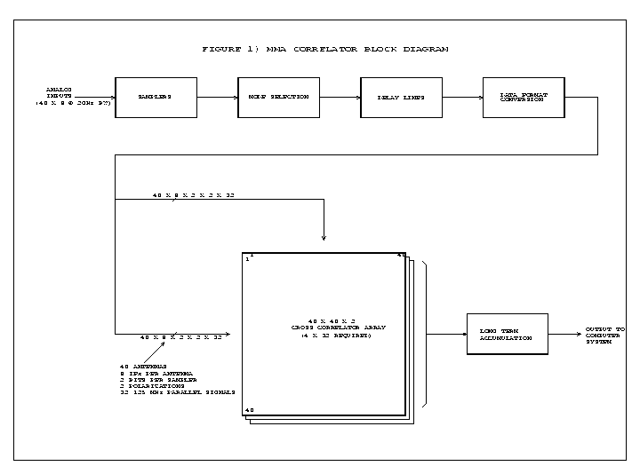
Figure 1:MMA Correlator Block Diagram.
Postscript version of Figure 1
may be easier to read.
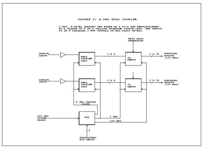
Figure 2:4 GHz Dual Sampler.
Postscript version of Figure 2
may be easier to read.
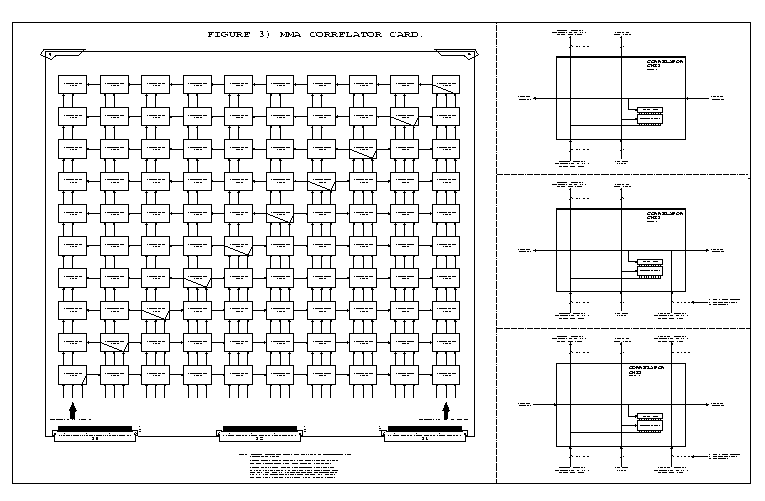
Figure 3:MMA Correlator Block Diagram.
Postscript version of Figure 3
may be easier to read.
11x17 postscript version of Figure 3
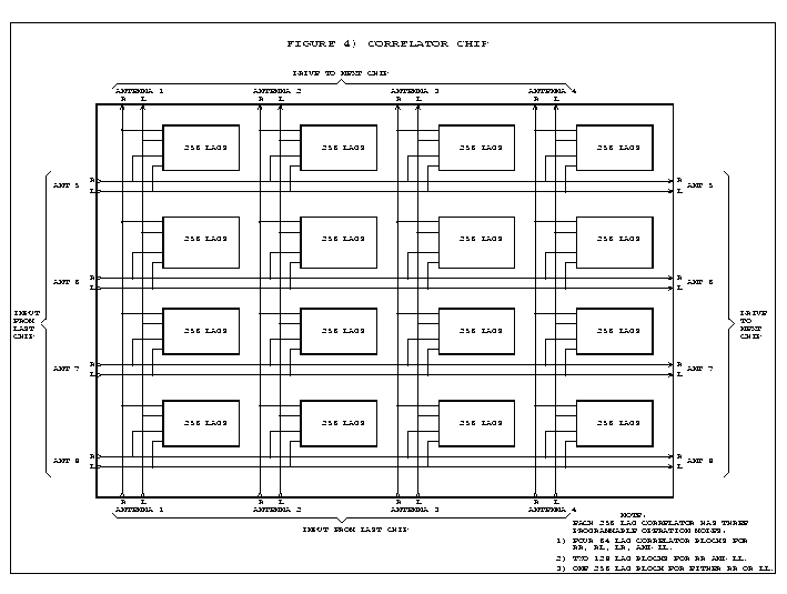
Figure 4:MMA Correlator Chip.
Postscript version of Figure 4
may be easier to read.