Back to Memolist
9th Int. Symp. on Space Terahertz Tech., March 17-19, 1998
MMA Memo 205:
A TUNERLESS SIS MIXER FOR 200 - 280
GHz WITH LOW OUTPUT CAPACITANCE AND INDUCTANCE
A. R. Kerr1, S.-K. Pan1,
A. W. Lichtenberger2 and H. H. Huang2
1National Radio Astronomy Observatory*
Charlottesville, VA 22903
2Department of Electrical Engineering**
University of Virginia
Charlottesville, VA 22904
ABSTRACT
The introduction by Padin et al. in 1996 of an SIS mixer with an integrated IF amplifier eliminates the need for an IF isolator and makes possible SIS receivers with multi-octave IF's. To realize a wide IF bandwidth, an SIS mixer must be designed with low IF capacitance and inductance. This paper describes an SIS mixer in which the RF circuit is effectively decoupled from the IF circuit, and a compact high-impedance RF choke circuit is used, resulting in low output capacitance and inductance.
INTRODUCTION
If an SIS receiver is operated with a 50-ohm
cable between the mixer and IF amplifier, impedance mismatch at the
ends of the cable can cause the overall receiver gain and noise
temperature to vary substantially across the IF band. This results
from two processes: (i) the IF signal from the mixer undergoes
multiple reflections between the mixer and amplifier, and (ii) the
outgoing noise wave from the input port of the amplifier is reflected
at the mixer and returns to interfere with the ingoing noise wave with
which it is correlated. An amplifier well matched to the cable
eliminates mechanism (i), while a well matched mixer eliminates both
(i) and (ii). In practice, SIS mixers do not usually operate with a
well matched output, and in many cases matching the output would lead
to undesirable behavior -- excessive conversion gain with a corresponding reduction of dynamic range, and negative RF input conductance which implies reflection gain at the mixer input. An isolator is often inserted in the cable, and presents a good match to both the mixer and amplifier. The isolator is not without penalty, however, as thermal noise from its internal termination is partially reflected at the mixer and adds to the IF noise; this can add significantly to the receiver noise temperature, even when the isolator is at 4 K. A more serious drawback may be the limited bandwith of an isolator, usually no greater than an octave. To achieve a wide IF bandwidth when using an isolator therefore requires a high IF center frequency. If it is desired to build a receiver with an IF bandwidth of 8 GHz, as is needed for the NRAO's proposed Millimeter Array, the use of an isolator would require an IF of 8-16 GHz IF, or higher.
The introduction by Padin et al. [1,2] of an SIS mixer with
a built-in IF amplifier makes possible SIS receivers with multi-octave
IF's, and eliminates the need for an IF isolator. It is pointed out in
[2] that to realize a wide IF bandwidth, the SIS mixer must be
designed with low output capacitance, and in general minimizing the
output circuit parasitics (capacitance and inductance) will facilitate
broadband coupling to the first IF stage. In many SIS mixers most of
the output capacitance is associated with the RF matching and choke
circuits, and the output inductance is mainly in the RF choke
circuit. In the present paper we describe an SIS mixer in which the RF
circuit is decoupled from the IF circuit, and a compact high-impedance
RF choke with low capacitance and inductance is used. The mixer
operates in the 200-280 GHz range, but the design is suitable for
scaling to higher or lower frequencies.
Three RF matching circuits used in SIS mixers are shown in
Fig.1. They are: (a) an end-loaded microstrip circuit, as used in
several very successful SAO mixers [3]; (b) a microstrip inductor
terminated with a
 RF/4 open-circuit microstrip stub, as used at NRAO
[4]; and (c), similar to (b), but with the microstrip inductor
terminated in a sectoral stub, as described in [5, 6]. As indicated in
the figure, for operation at ~230 GHz, the static (low frequency)
capacitance of the three circuits is between 200 and 500 fF.
RF/4 open-circuit microstrip stub, as used at NRAO
[4]; and (c), similar to (b), but with the microstrip inductor
terminated in a sectoral stub, as described in [5, 6]. As indicated in
the figure, for operation at ~230 GHz, the static (low frequency)
capacitance of the three circuits is between 200 and 500 fF.
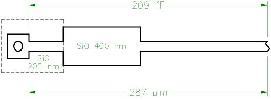
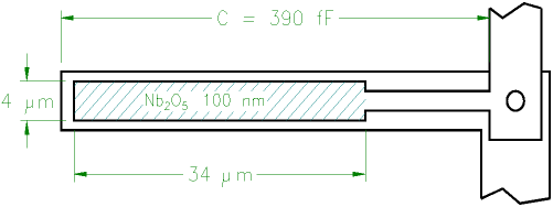
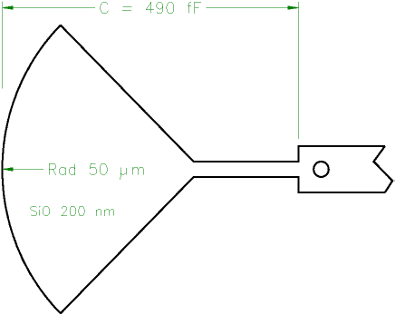
Fig. 1. Three RF tuning circuits used in SIS mixers. Dimensions and
capacitances indicated are for a center frequency of ~230 GHz. (a) End
loaded matching circuit. (b) Tuning inductor with /4 microstrip stub.
(c) Tuning inductor with radial microstrip stub. (Diagrams not to scale.)
For the SAO mixer complete with RF chokes, the static capacitance at the IF port is 470 fF. This consists of 200 fF from the RF choke, 210 fF from the RF matching circuit, and 60 fF from the SIS junction itself. The low-frequency inductance of the IF circuit is 1700 pH, of which only 42 pH is from the RF matching circuit.
A NEW DESIGN
It is clear from the foregoing that to reduce the IF output
capacitance of an SIS mixer, the capacitance of the RF matching
circuit and/or the RF choke must be reduced. The IF inductance can be
reduced by reducing the inductance of the RF choke. A design which
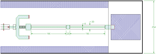
attempts to minimize both these components is shown in Fig.2. The
mixer is fabricated on a 0.010" fused quartz substrate, thinned after
lithography to 0.0035". A 50-ohm suspended stripline, at the left end
of the substrate in Fig. 2(a), is driven by a broadband transition [7]
from full-height rectangular waveguide. Near the middle of the
substrate is a broadband transition from suspended stripline to
capacitively loaded coplanar waveguide (CLCPW) [8]. This transition is
almost identical in geometry to the suspended stripline-to-coplanar
waveguide (CPW) transition described in [7]. The CLCPW has a
characteristic impedance of 63 ohms, and is the first element of the
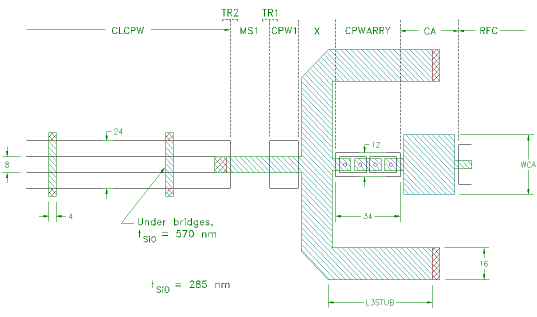
broadband RF matching circuit -- see Fig. 2(b). The next matching elements are short sections of microstrip and CPW in series, followed by a parallel pair of quarter-wave short-circuit microstrip stubs of characteristic impedance 3.4 ohms. The series array of four SIS junctions is connected through a capacitor (CA) to ground, and to a high impedance RF choke (RFC) as shown in Fig. 2(c). Note that all conductors are on the same side of the substrate. The ground plane extends over most of the right half of the substrate and has gold pads along the edges (indicated in Fig. 2 by heavy hatching) which make contact with the shoulders of the substrate channel via 0.001" gold crush wires.
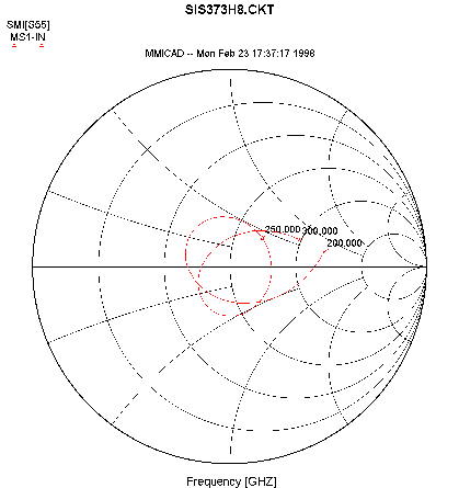
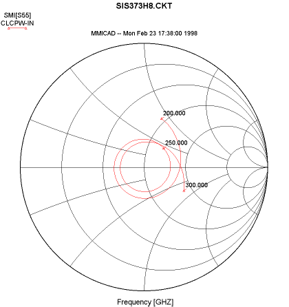
Operation of the RF tuning circuit is as follows: The series array
of four SIS junctions is inductive and is resonated by capacitor
CA to ground. Its input impedance, as seen from the stubs,
is plotted as a function of frequency in Fig. 3(a). Adding the stubs
winds up the impedance locus as in Fig. 3(b). The microstrip MS1 and
the coplanar line CPW1 form a resonant LC transformer which increases
the impedance level to about 50 ohms, as in Fig. 3(c). Finally, the
CLCPW, which has an electrical length of about half a wavelength,
transforms the locus as in Fig.3 (d). The parameters assumed in these
simulations are: junction diameter a = 1.5 µ m, critical current density JC
= 6600 A/cm2, and specific capacitance CS = 85
fF/µm2, corresponding to a normal resistance
RN = 15.5 ohms per junction and  RNCJ = 3.6 at 250
GHz.
RNCJ = 3.6 at 250
GHz.
The RF choke, shown in Fig. 2(c), is designed to present a high RF impedance to the array of SIS junctions and capacitor CA. It has two sections, each consisting of a CPW of 110-ohm characteristic impedance followed by a capacitor to ground, and has a total static capacitance of 137 fF and inductance of 235 pH. In most applications one section (line + capacitor) can be omitted, which reduces the capacitance to 68 fF and inductance to 118 pH.
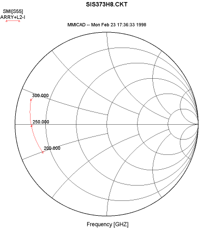
The RF embedding impedance seen by each junction in the array is shown
in Fig. 4. The Smith chart is normalized to the optimum source
impedance1 for the junctions, 12.5 ohms (per junction) in
the present case. The junction capacitance is included as part of the
embedding circuit in this calculation. The circle at | | = 0.4 indicates the range of embedding impedances within which acceptable SIS mixer performance will be obtained [11].
To accommodate variations from wafer to wafer, particularly in JC, junction area, and SiO thickness, each wafer contains twelve mixer designs with four values of WCA and three values of L3,STUB (see Fig. 2(b)).
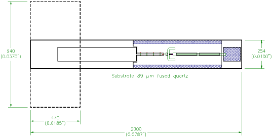
(a)
(b)
(c)
Fig. 2. Diagrams of the low-parasitic mixer. (a) The whole mixer, showing the suspended stripline probe which couples to the signal/LO waveguide at the left. The ground plane contacts the mixer block along gold plated contact strips, shown heavily hatched on the upper and lower edged of the substrate. The bonding pad for the IF connection is at the right end of the substrate. (b) The RF tuning circuit, showing the end of the CLCPW (at the left), microstrip and CPW (capacitive and inductive) lines, the pair of microstrip short-circuit stubs, series array of four SIS junctions, and tuning capacitor CA. (c) The right-hand end of the substrate, showing the RF tuning circuit at the left, the two-section RF choke, and the DC/IF bonding pad.
(a)
(b)
(c)
(d)
Fig. 3. RF impedance transformation through the broadband matching network. (a) Impedance of the array of junctions and capacitor CA, (b) including the two stubs, (c) including MS1 and CPW1, and (d) including the CLCPW input line. All Smith charts are normalized to 50 ohms.
At IF, the pair of microstrip stubs has a very low impedance to
ground, effectively bypassing the rest of the RF matching circuit. The
static capacitance of the whole mixer, seen at the IF port on the
substrate, is 241 fF, which consists of contributions from the array
of junctions (38 fF), the tuning capacitor CA (66 fF), and
the RF choke (137 fF). The corresponding low frequency inductance is
294 pH of which 59 pH is contributed by the RF matching circuit. If
only a single section RF choke is used, the overall static capacitance
and inductance are reduced to 172 fF and 174 pH.
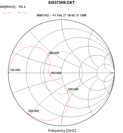
Fig. 4. RF embedding impedance seen by the array. The junction
capacitance is taken as part of the embedding circuit. The circle is
at || = 0.4. (The Smith chart is normalized to the optimum source impedance.)
FABRICATION
The mixers were fabricated on chemically polished fused quartz wafers 1" diameter and 0.010" thick. After dicing the individual mixers were thinned to 0.0035" using a dicing saw. The new mixer differs in three ways from those previously made at UVA: (i) the junctions are situated on small islands of trilayer where it is not possible to use removable anodization lines, (ii) an SiO layer 200 nm thick is deposited around the junctions, with a thicker SiO layer in the CLCPW sections, and (iii) vias are required to connect the bridges in the CLCPW section to the base electrode. Our previously established Cr based trilevel resist [12] and Futurex junction anodization [13] processes were inadequate for requirements (i) and (ii). For the present mixers we adapted JPL�s Au overlayer technique [14] to our processes. Since Au does not naturally oxidize, an in-situ physical cleaning of the surface of the junction counter electrode is not needed prior to depositing the Nb interconnection layer. Omitting the usual physical cleaning step has two advantageous: any native Nb and Al oxides which have grown after deposition of the junction SiO insulation will remain, and the SiO insulation layer will not be disturbed. Both these factors tend to prevent micro-shorts between the wiring and base electrodes, and we have been able to fabricate junctions with 200 nm insulation layers without resorting to anodization techniques.
In the Au overlayer process we used a separate DC magnetron sputtering
system to deposit layers of Au(1-2 nm)/[Cr(4% wt.)-Au](28 nm) on top
of the trilayer wafer after an ion gun clean. The Cr-Au mixture was
used to increase the physical durability of the over-layer. Prior to
the trilayer etch, the Cr-Au layer is etched in a solution of 10 g I,
40 g INH4 , 400 ml DI water, and 600 ml ethanol, which we
have found etches Cr-Au films containing as little as 0.4% (wt.) Cr
more repeatably and uniformly than pure Au films. Before the junction
etch, the Au/Cr-Au layer is removed with an ion beam inclined at
45� which cleans the surface around the perimeter of the polyimide etch mask. After the junction etch and SiO deposition, a liftoff of the self-aligned trilevel resist is performed. It was found that the (CH3 )4 NO4 in our usual 300T resist stripper attacked the counter electrode/overlayer interface, resulting in the loss of the Au/Cr-Au overlayer from the tops of the small junctions. The 300T stripper was replaced with OCG Inc. QZ-3321 or NMP, both of which have been found satisfactory.
The vias, to connect the bridges in the CLCPW section to the base electrode, can be accomplished in two ways. The first is to use large area junctions, and the second uses a direct contact from counter electrode to base electrode. We have chosen the second approach to avoid possible internal resonances in large-area junctions used as vias. Since an in-situ cleaning step is not used in our Nb wiring process, a second Au overlayer was defined on top of the base electrode after removing the Au/Cr-Au and Nb counter electrode from the via sites.
INITIAL RESULTS
The mixer described here had a normal resistance of 93 ohms for the
array of four junctions, and the junction diameter, measured by SEM,
was 1.6 µm, corresponding to a critical current density of 3900
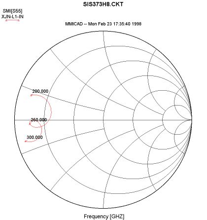
A/cm2 and RNCJ = 6.2. The I-V curve at 4.2 K is shown in Fig. 5 with and without LO power applied. With appropriate choice of tuning elements CA and L3,STUB, the embedding impedance seen by the array is as shown in Fig. 6, in which impedances are normalized to the optimum source impedance for this particular mixer (74 ohms).
The mixer was tested in a liquid helium cooled vacuum cryostat
containing 4.2 K IF calibration components, similar to that described
in [15]. The incoming RF signal enters the cryostat through a plastic
film vacuum window supported by polystyrene foam [16]. It passes
through a PTFE infrared filter at 77 K into a scalar feed horn at 4.2
K. LO power is injected through a 20 dB branch-line directional
coupler, also at 4.2 K. A 50-ohm 1.4 GHz IF was used with a 50-MHz
bandwidth and no IF impedance transformer between the mixer and
amplifier. The IF noise temperature, including a coaxial switch, two
isolators, and a directional coupler, was 6.3 K. A DC magnetic field
was applied to the mixer to suppress the Josephson currents in the
junctions.
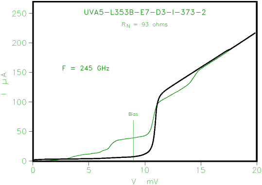
Fig. 5. I-V curve for the mixer at 4.2 K without LO power (heavy line), and with LO power at 245 GHz (light line). The operating bias voltage is indicated by the vertical line.
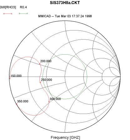
Fig. 6. RF embedding impedance seen by the array. The junction
capacitance is taken as part of the embedding network. The circle is
at || = 0.4. The Smith chart is normalized to the optimum source impedance (74 ohms).
The overall receiver and mixer noise temperatures are plotted as
functions of LO frequency in Fig. 7. The mixer noise temperature
includes contributions from the vacuum window, IR filter, horn, and LO
coupler, but does not include contributions from the IF amplifier,
reflected noise from the termination on the IF isolator, or injected
noise from the LO. Fig. 8 shows the mixer conversion loss and VSWR at
the IF port of the mixer (with respect to 50 ohms) as functions of LO
frequency . The conversion loss includes contributions from the vacuum
window, IR filter, feed horn, and LO coupler.
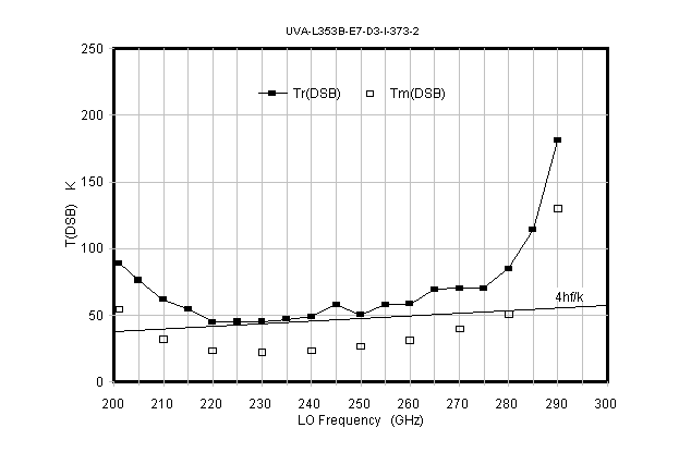
Fig. 7. DSB receiver noise temperature (solid line) and mixer
noise temperature (open squares). Shown for reference is the line
4hf/k.
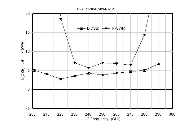
Fig. 8. DSB conversion loss (lower curve) and IF port VSWR.
CONCLUSION
The new mixer has output capacitance and inductance lower by factors
of about 2 and 6 than typical SIS mixers in this band. These
parasitics could be further reduced by using a single-section RF choke
as discussed above. The initial measurements presented here gave
overall receiver noise temperatures of 45 - 89 K (DSB) over the LO
range 200 - 280 GHz, with corresponding mixer noise temperatures of 22
- 55 K (DSB). By increasing the critical current density of the junctions to ~6600 A/cm2 we hope to improve the performance and cover the full 200-300 GHz band.
We have not yet operated this type of mixer with an internal
wideband IF amplifier, but only with an L-band IF. While the present
mixer operates in the 200 - 300 GHz waveguide band, the design should be suitable for scaling to higher or lower frequencies. Note that, with frequency scaling, the IF output capacitance and inductance will change, both increasing as the design is scaled to lower frequencies.
ACKNOWLEDGMENTS
The authors thank R. Amos for his help in fabricating the niobium circuits, N. Horner, F. Johnson, and A. Marshall for fabricating and assembling the mixer, and K. Crady for his help in testing the mixer.
REFERENCES
[1] S. Padin, "An Integrated SIS Mixer and HEMT IF Amplifier," National Radio Astronomy Observatory, Millimeter Array Memo No. 114, April 1994.
[2] S. Padin, D. P. Woody, J. A. Stern, H. G. LeDuc, R. Blundell, C.-Y. E. Tong, and M. W. Pospieszalski, "An Integrated SIS Mixer and HEMT IF Amplifier" IEEE Trans. Microwave Theory Tech., vol. MTT-44, no. 6, pp. 987- 990, June 1996.
[3] R. Blundell, C.-Y. E. Tong, D. C. Papa, R. L. Leombruno, X. Zhang, S. Paine, J. Stern, H. G. LeDuc, and B. Bumble, "A wideband fixed-tuned SIS receiver for 200 GHz operation," IEEE Trans. Microwave Theory Tech., vol. MTT-43, no. 4, pp. 933-937, April 1995.
[4] A.R. Kerr, S.-K. Pan, and M. J. Feldman, "Integrated tuning elements for SIS mixers," Int. J. Infrared Millimeter Waves, vol. 9, no. 2, pp. 203-212, Feb. 1988.
[5] G. Pance and M. J. Wengler, "Integrated tuning elements for millimeter and submillimeter SIS mixers," IEEE International Microwave Symposium Digest, pp. 337-340, June 1992.
[6] J. Zmuidzinas and H. G. LeDuc, "Quasi-optical slot antenna SIS mixers," IEEE Trans. Microwave Theory Tech., vol. 40, no. 9, pp. 1797-1804, Sep. 1992.
[7] A. R. Kerr, S.-K. Pan, S. Whiteley, M. Radparvar, and S. Faris, "A Fully Integrated SIS Mixer for 75-110 GHz," IEEE Int. Microwave Symp. Digest, pp. 851-854, May 1990.
[8] A. R. Kerr and S.-K. Pan, "Design of planar image-separating and balanced SIS mixers, Proceedings of the Seventh International Symposium on Space Terahertz Technology, pp. 207-219, 12-14 March 1996. (Also available on the web at http://www.mma.nrao.edu/memos/memolist.html. as Millimeter Array Memo. 151.)
[9] A. R. Kerr, S.-K. Pan, A. W. Lichtenberger and D. M. Lea, "Progress on Tunerless SIS Mixers for the 200-300 GHz Band," IEEE Microwave and Guided Wave Letters, vol. 2, no. 11, pp. 454-456, Nov. 1992.
[10] Q. Ke and M. J. Feldman, "Optimum source conductance for high frequency superconducting quasiparticle receivers," IEEE Trans. Microwave Theory Tech., vol. MTT-41, no. 4, pp. 600-604, April 1993.
[11] A. R. Kerr, "Some fundamental and practical limits on broadband matching to capacitive devices, and the implications for ShhIS mixer design," IEEE Trans. Microwave Theory Tech., vol. MTT-43, no. 1, pp. 2-13, Jan 1995.
[12] A.W. Lichtenberger, D. M. Lea, C. Li, F. L. Lloyd, R. J. Mattauch, M. J. Feldman, S.-K. Pan, and A. R. Kerr, "Fabrication of Micron Size Artificially Insulated Nb/Al-Al2O3 /Nb Junctions with a Trilevel Resist Liftoff Process," IEEE Trans. Magn., MAG-27(20), March 1991.
[13] D. M. Lea, H. H. Huang, and A.W. Lichtenberger, "Use of a Negative Tone Photoresist to Improve Low-Tc Superconducting Tunnel Junction Fabrication Processes", IEEE Transactions on Applied Superconductivity, 1997.